
For my mixed-signal VLSI course, a partner and I were tasked with designing and laying out a 7-Bit DAC using a MOSFET ladder network. We needed to meet several performance and operation requirements - the DAC needed to function for a range of supply and output voltages while maintaining good linearity.
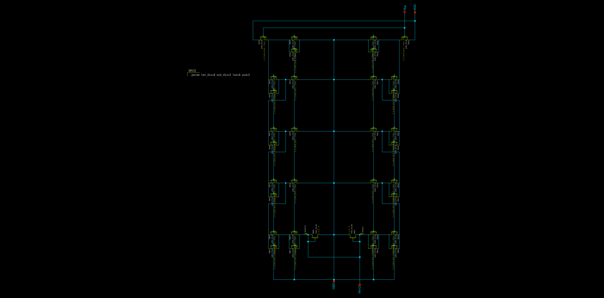
To start the design process, we chose a simple ladder network that was provided as a starting point. This ladder doesn’t have particularly strict output voltage requirements, as the output transistor just needs to be held in saturation for proper operation. This is useful because mirroring the output current does require some voltage on that node below VDD.
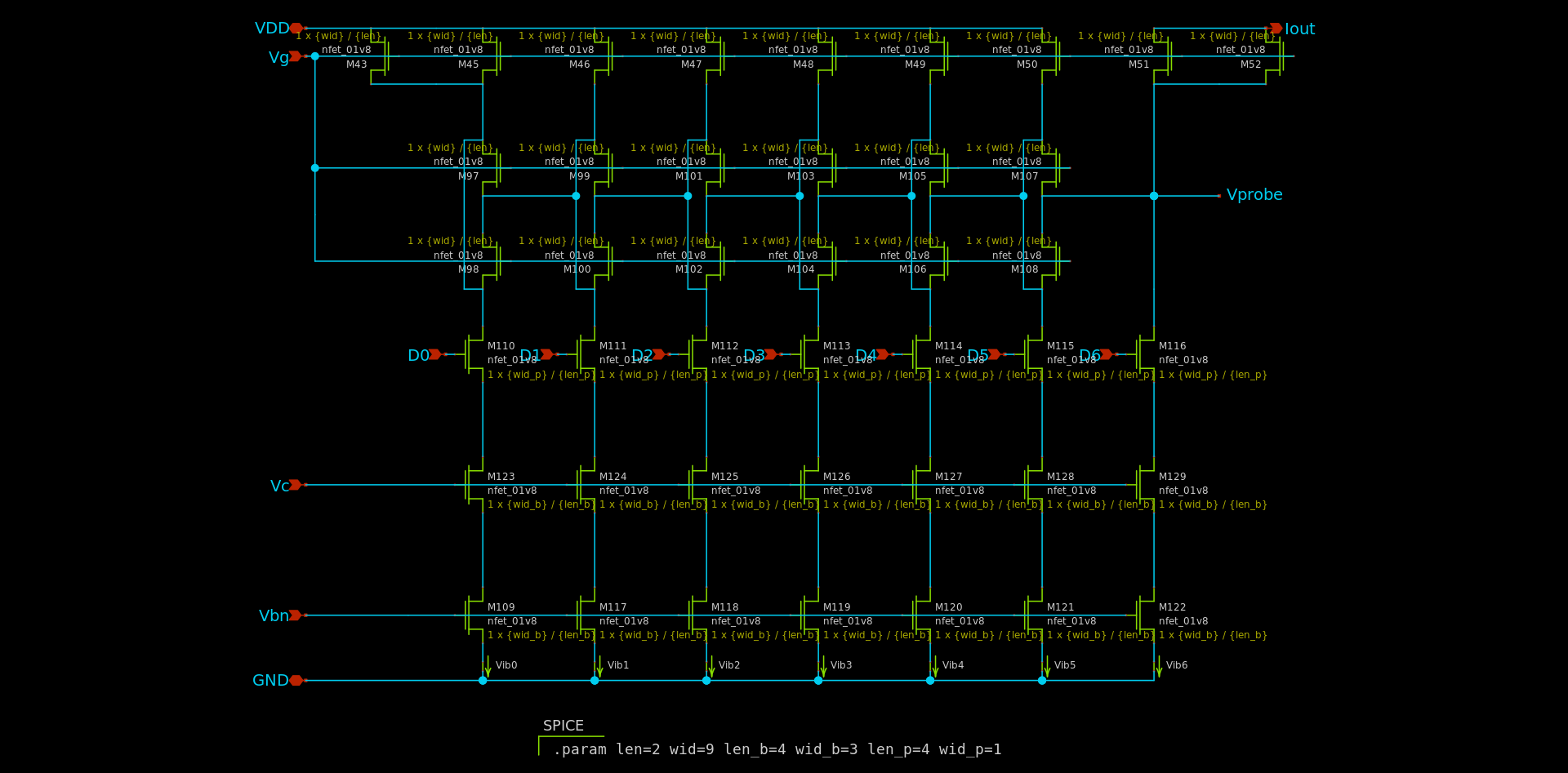
To make the switched current sinks, we added pass transistors which connect to the DACs digital inputs in series with cascoded bias transistors. An unforeseen consequence of this implementation is that because the cascoded bias transistors also have to remain above saturation to properly sink our bias current, our input voltage requirement for the next stage becomes stricter. Despite this, we still decided to cascode the bias transistors because it helped mitigate the Early effect, improving matching.
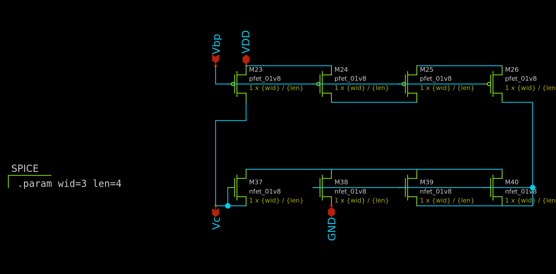
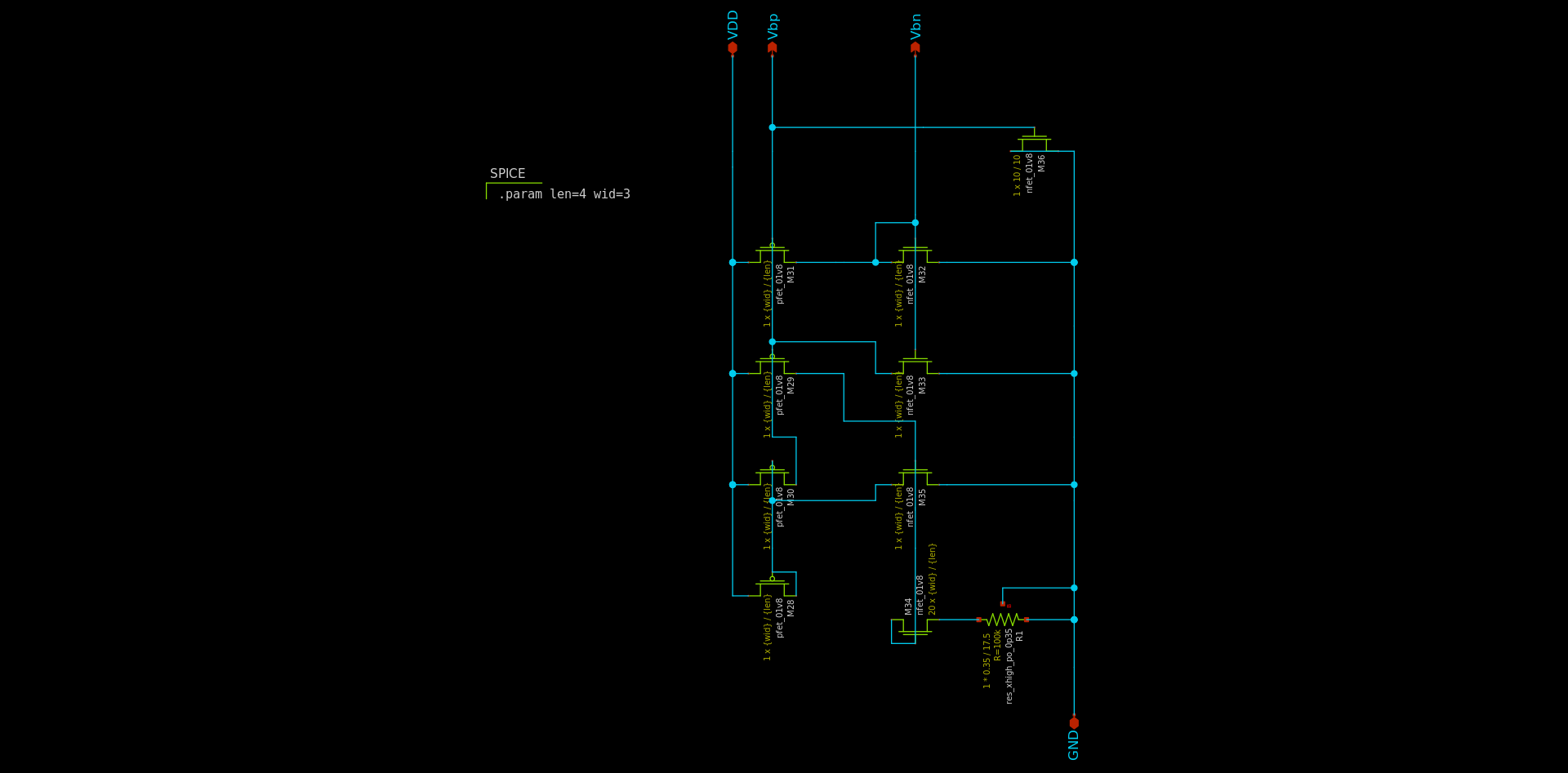
To generate the cascode bias voltage (Vc), we used a cascode bias circuit
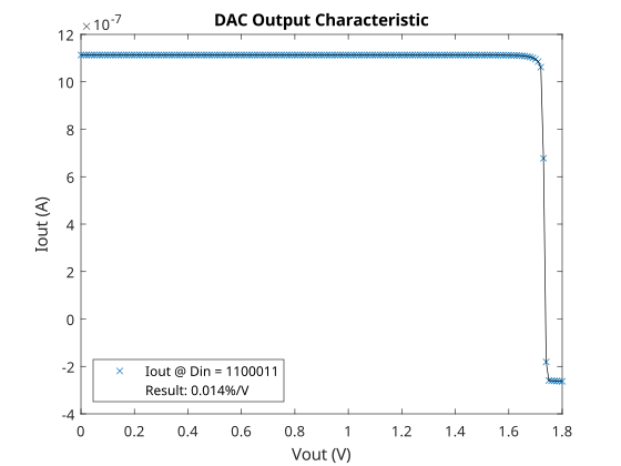
One requirement of our DAC is that it has to have less than a 0.5%/V change in Iout as Vout is swept over at least 80% of the power supply range. In order to do this, we needed to mirror the output current from the ladder. We chose to implement a PMOS version of the Cong and Geiger Mirror.
This Mirror features an extremely flat output characteristic and a low input voltage requirement (around Vdssat), making it a reasonable choice. The design generates its own PMOS cascode bias voltage.
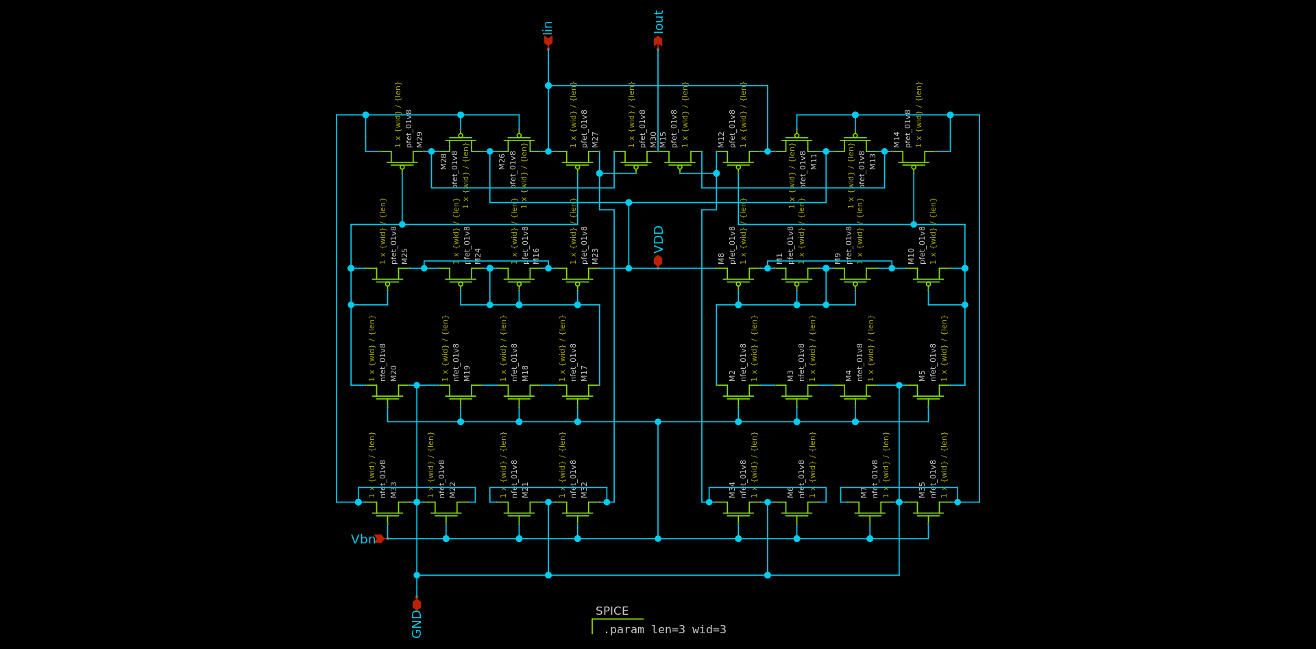
This current mirror does require an external bias, and it mirrors best when the bias is at least several times smaller than the input. Because of how the ladder operates, this means that we needed to divide down the bias current. We used the same principle as the ladder to create a 1/24 ratio.
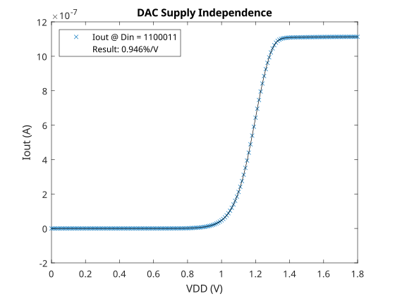
Another requirement of our DAC is that it has to have less than a 0.5%/V change in Iout for the range that it operates when VDD is swept. In other words, we needed supply-independent biasing. We ended up using the so-called ”Magic Circuit” we covered in class.
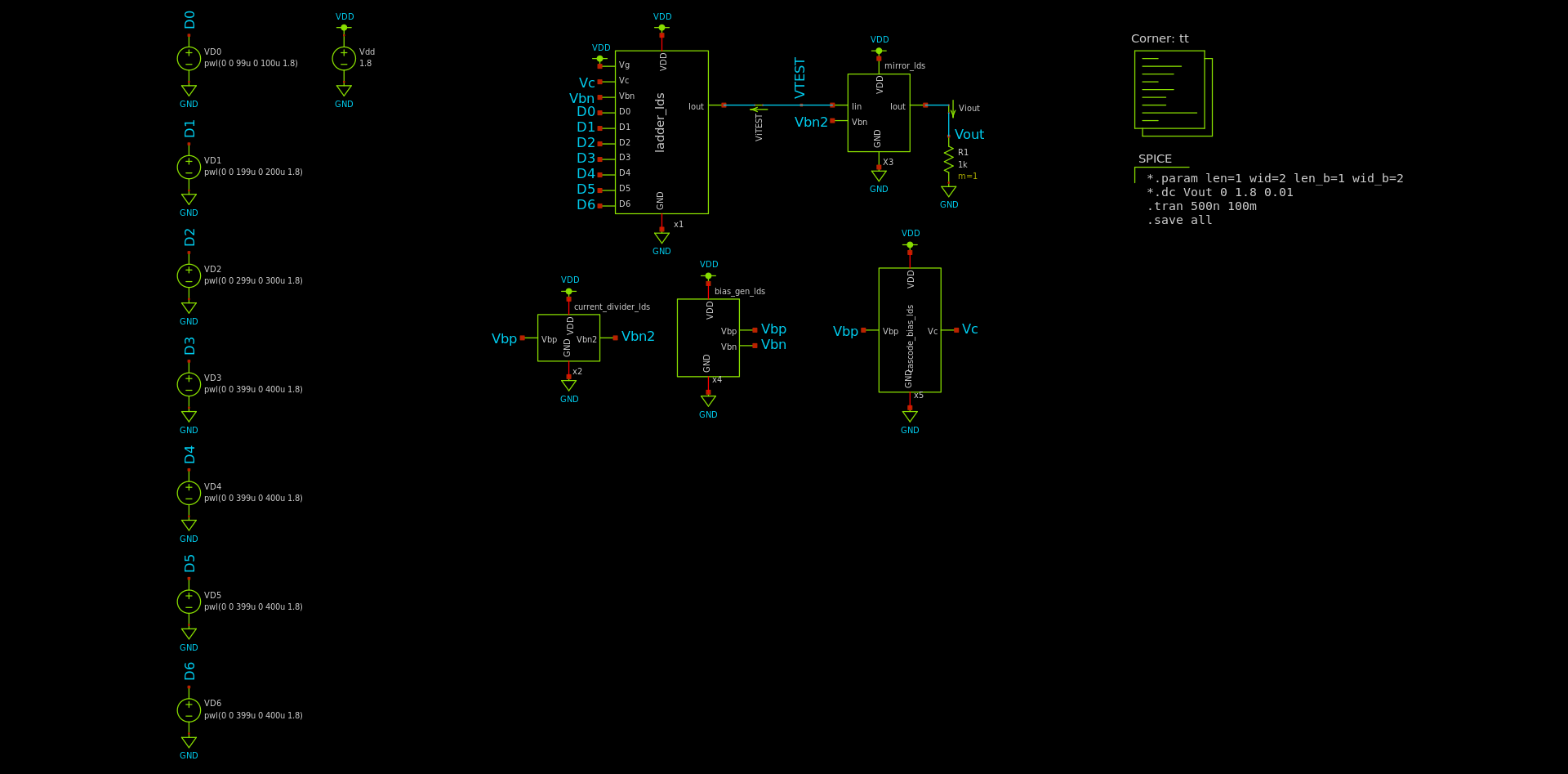
With all of these components, we created a hierarchical schematic of our DAC. We ran extensive transient simulations to ensure stability.
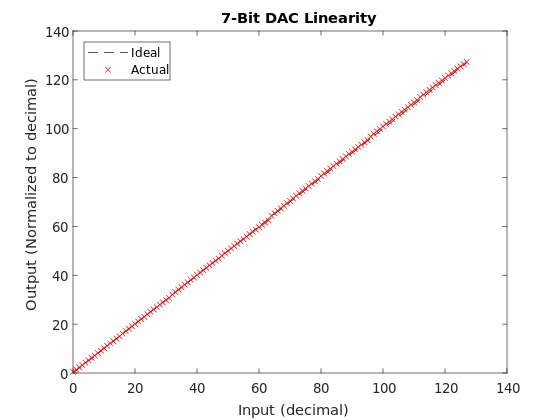
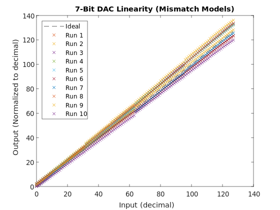
Using a similar testbench, we looked at the output current for every digital input. We then normalized the output based on our bias current, allowing us to compute the DNL and INL of our DAC in terms of LSBs. The DAC needed to have less than 2 LSBs of DNL and less than 4 LSBs of INL.
For the TT corner, we achieved a DNL of 0.94 LSBs and an INL of -0.20 LSBs.
Another requirement, which was particularly difficult, was to hit less than 8 LSBs of DNL/INL while using the mismatch models. We managed to achieve this in a run of 10 monte-carlo simulations.
To satisfy the operating requirements, we swept Vout, and we found that there is a 0.014%/V change in Iout over 80% of the power supply range.
To prove supply independence, we swept VDD and we found that for the range that the DAC operates in (about 1.4V - 1.8V), there is a 0.946%/V change in Iout.
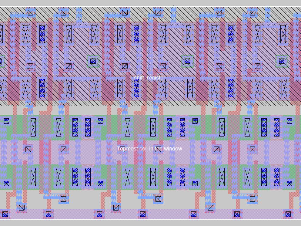
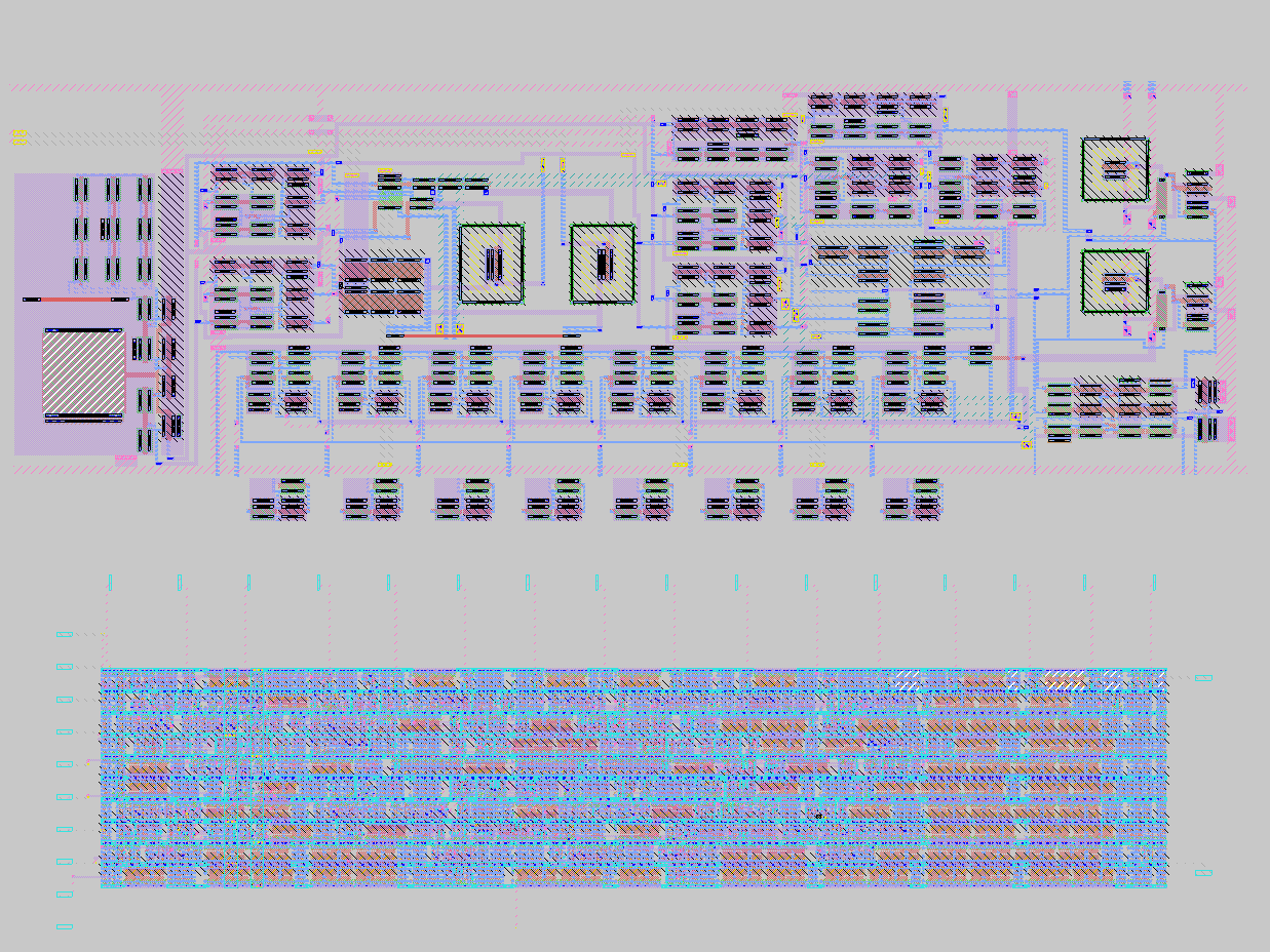
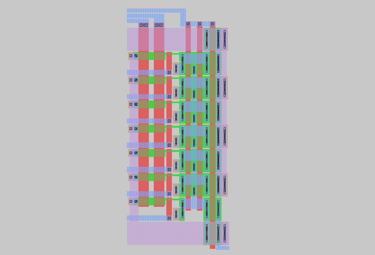
We used several best-practice analog layout techniques to minimize device mismatch. In general, we used fairly large transistors (several square microns in area) and minimized spacing in between devices.
The mirror and the current divider (left and right respectively) utilize common-centriod geometry to compensate for linear gradients.
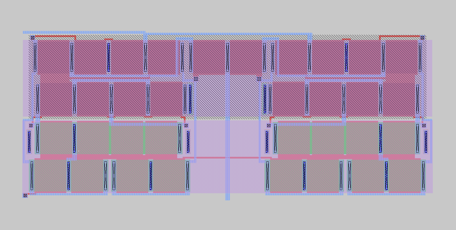
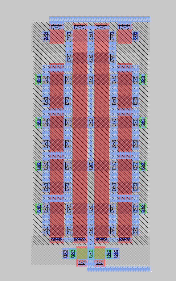
The ladder, cascode bias, and bias generator (left, right, bottom) all have their devices in the same orientation.

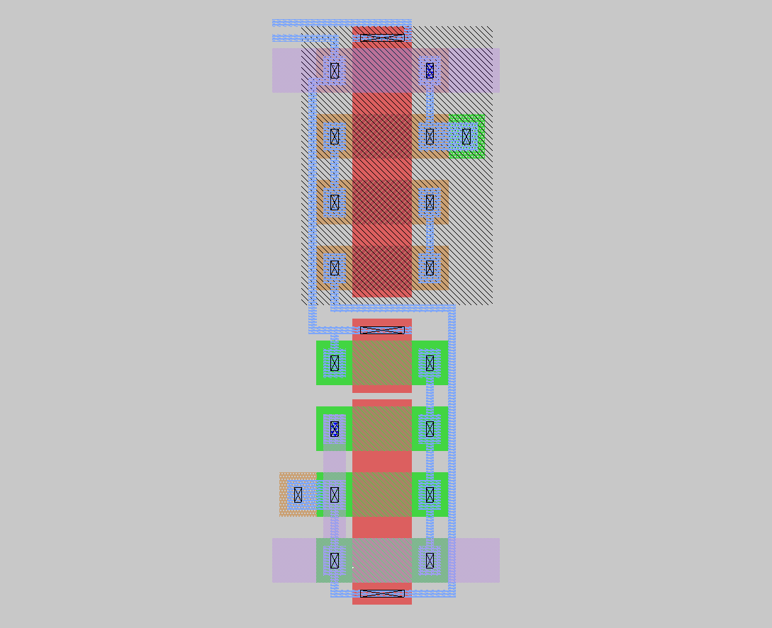
For the bias generator, we decided to use one of the P- precision resistors described here. This was kind of annoying to get working because for whatever reason it doesn’t work the same as it did 4 years ago. We found this video helpful in fixing DRC.
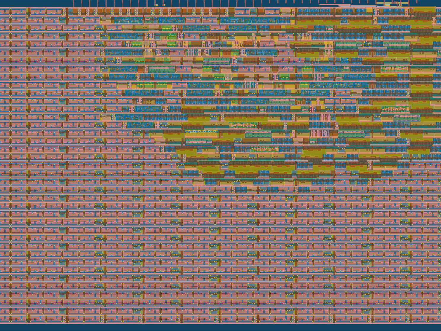
Lastly, we connected all of our components. Something that we would probably change if we had more time was consistency in layout. It’s pretty easy to tell who did what block and there’s clearly some issues in our cell I/O that could have been optimized further. Regardless, here is our final DAC layout:
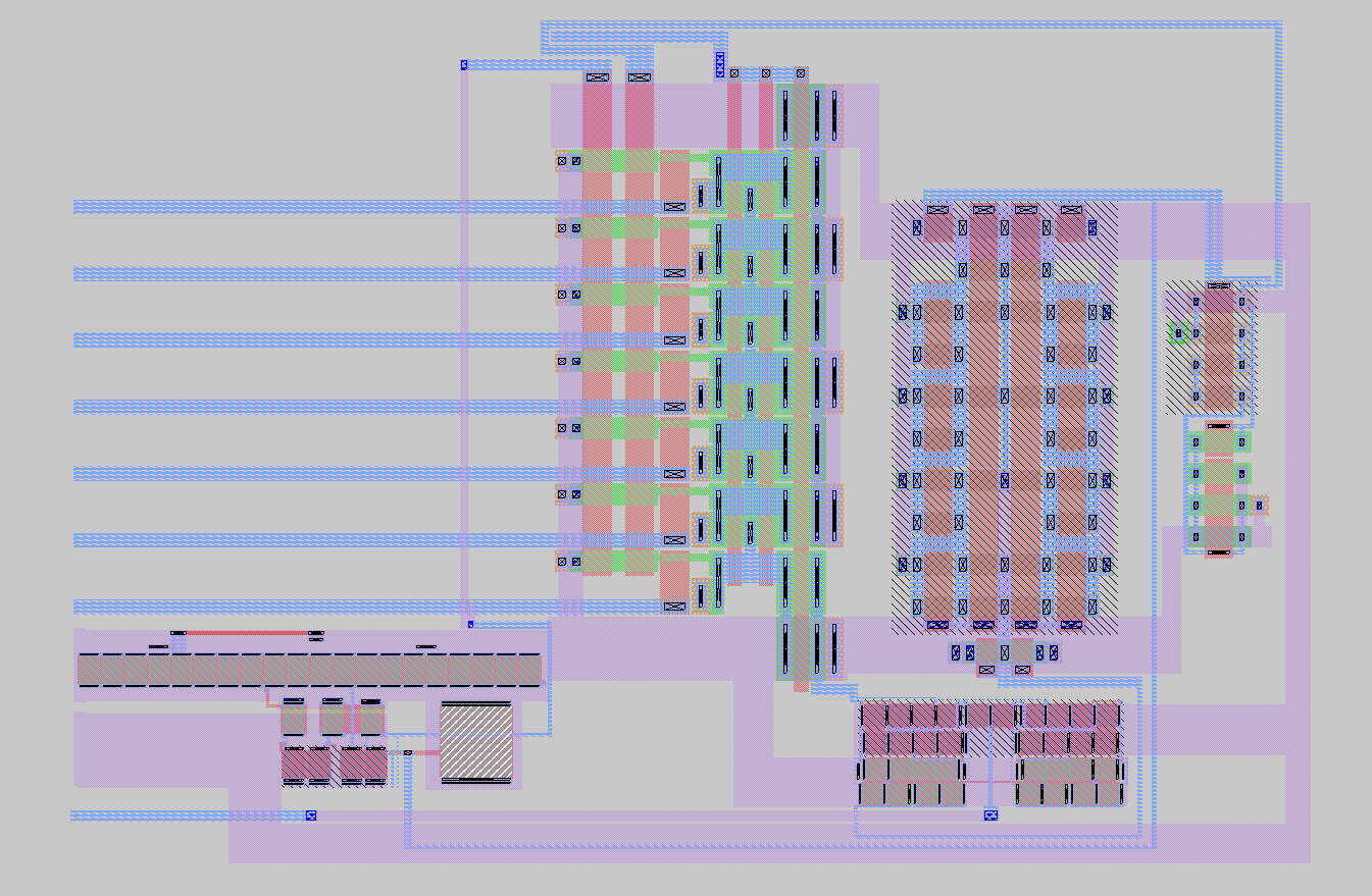
We verified our design using netgen LVS, proving that we had implemented the DAC correctly.
On a candid note, this was by far the most effort I've ever put into a project. I spent so much time on the design and simulation - it was incredibly difficult to get us in spec with the mismatch models while making sure the output was stable. I hope this writeup serves as a good overview of what I can do in the mixed-signal design space. Thanks for reading!